PCB Assembly

Asia Pacific Circuits offers One-stop Electronics Manufacturing Services located in Shenzhen, China. We handle the whole process including Printed Circuit Board Assembly, PCB Manufacturing, Components Sourcing, IC Programming, PCBA Testing, Box Build Assembly, Logistics, Packing and etc.

Our 4,000㎡ smart workshop owned global advanced equipment which including Panasonic (NPM-D3) & Hanwha (DECAN S2) automatic high-speed precision placement machines, German ERSA (3/45) vacuum reflow soldering & Selective wave soldering, solder paste viscosity detector, 3D-SPI, 3D-AOI, 3D offline & online X-ray, BGA automatic precision rework station, 3D printer, automatic conformal coating machine, laser marking machine, automatic software burning equipment and so on.

Mounting component size from 01005 package to 100*90*21mm (IC size). Mounting accuracy: ±0.035mm (repeat positioning accuracy ±0.025mm) Cpk≧1.0 (3σ). 0201 package and pitch 0.2mm BGA placement capabilities very mature. We also have mature lead-free soldering process technology.

Our company covers many areas such as Industrial Automation Control, Artificial Intelligence, Robotics, Automotive Electronics, Medical Electronics, Smart Home, Security System, etc. To offer premium PCB Assembly Service to our customers is always our pursuit.

WHY CHOOSE APC AS YOUR PCB ASSEMBLY MANUFACTURER?

Strict Quality Control

We are a PCB assembly factory in China since 2004. We focus on middle and high-end complete turnkey PCB assembly. 99.9% pass rate.

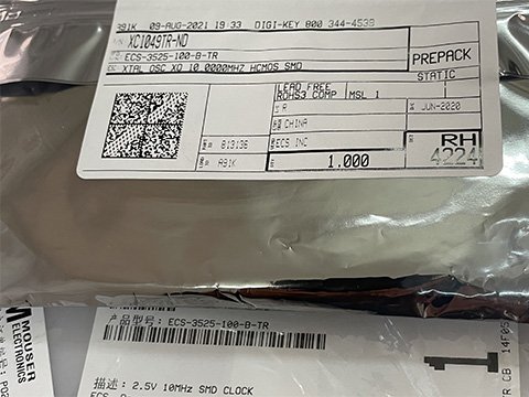
Original Parts Sourcing

We source the electronic components from big trader or original manufacturers. Distributors such as Future, Avnet, Arrow, Master, Digi Key, Mouser and so on.

Solder Paste Storage

We pay high attention to the management of solder paste and we have introduced a constant temperature management alarm system.

Parts Pre-baking

In order to improve the soldering reliability, we have dedicated oven for PCB & component pre-baking.
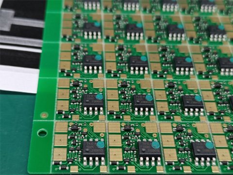
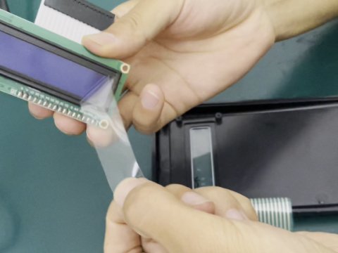
Inspection

We do visual inspection, AOI inspection, x-ray inspection. QC strictly enforces the standards: IPC II and IPC III.
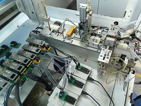
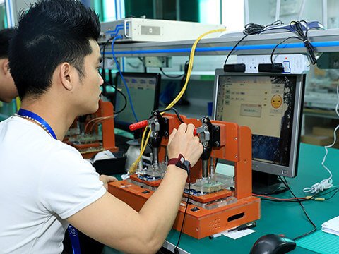
Programming and FCT

We provide programming and FCT (function test) services to ensure that every product you receive is qualified.

Component Storage

We attach great importance to component storage. Such as temperature and humidity control and first-in-first-out mechanism.
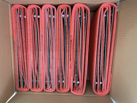
Reliable Packaging

We provide customized packaging solution to ensure your boards arrive you safely.

On-Time Delivery

We implement MES electronic information board to supervise the PMC production plan so we can deliver the product timely.

WHAT WE CAN DO OF PCB ASSEMBLY SERVICES ?

APC engineer team analyze Gerber file for you carefully after order placed. For example, to avoid bending or breaking we will pay attention to the relationship between the hole spacing of the PCB and the bearing capacity of the board. We will also check if the PCB layout takes into account key factors such as high-frequency signal interference and impedance.

HASL-PCB-Fabrication
Original parts sourcing

We strictly control the component channels for our customers. To avoid second-hand or fake raw materials we purchase the electronic components mainly from big traders or original manufacturers. Distributors such as Future, Avnet, Arrow, Master, Digi Key, Mouser and so on. In addition, we inspect the key incoming materials strictly such as chips then ensure the components are free from failure.

  • Surface Mounting Technology (SMT)

Solder paste printing and reflow oven temperature control are key points, and qualified laser stencils which meet process requirements are also very important. According to the requirements of the PCB, some pads need to increase or reduce the size of the stencil hole or use U-shaped holes. We make the stencil according to the process requirements. The temperature and speed control of reflow soldering is critical for solder paste wetting and soldering reliability. We follow the SOP operation guidance. In addition, AOI detection needs to be strictly implemented to minimize the adverse effects caused by human factors.

Surface Mounting Technology
A PCB board assembled by THT
  • THT Through Hole Technology

Mold design for wave soldering is a key point. It’s very important that how to use the mold which can maximize the qualified products after furnace. This is a process that PE engineers must constantly practice and sum up experience.

  •  Programming

In the DFM report, we would recommend setting some test points to test the board and test the continuity of the PCBA after circuit card assembly. If possible, please provide the program, and download the program into the main control IC through a programmer, so that we can test functional changes by various touch actions directly to verify the functional integrity of the entire PCBA.

IC Programming
PCBA TEST FCT
  • PCBA Test

We can help our clients to test PCBA if requested which including ICT, FCT, aging test, temperature test, humidity test, drop test, etc. It depends on client’s testing requirements.

  • Finished Product Assembly

Our manufacturer not only offer circuit card assembly service, but can help you to achieve finished product assembly as well. You can purchase all parts (for example, housing or LCD screen) by your side and just send us before assembly or we can also purchase for you. We have rich experience to cooperate with excellent mold factories for many years.

Finished assembly case of LCD screen
Circuit Card Assembly Packing
  • Packing and Shipping

We can help you finish packing and shipping after production completed. Inner box and carton box can be customized. We pack all boards with suitable box. You just tell us by air transport or ocean shipment. Full shipment or partial shipment both available. We can offer a free storage fee only if the products stay in our warehouse not over 3 months.

CAPABILITIES OF PRINTED CIRCUIT ASSEMBLY

CapabilityStandard
Parts Procurement:Full Turnkey, Partial Turnkey
Types of Assembly:Surface Mount (SMT), Thru-hole, Mixed Technology, Single and double-sided SMT/PTH.
Stencils:Laser cut stainless steel and Nano-coating
Components:Passive components smallest size 01005, Fine pitch components smallest size 14 Mils pitch.
Component Packaging:Reels, Cut tape, Tube and tray, Loose parts and bulk
Testing Procedures:Visual inspection, X-ray Inspection, AOI (Automated Optical Inspection), ICT (In-Circuit Test), Functional testing
Solder Type:Leaded and Lead-free/ RoHS compliant
Assembly Surface Mount Connectors:Yes
Wave Soldering:Yes
PCB Dimensions:Largest size: 23.6″ x 35.4″ (600mm x 900mm)
Panelized PCB:Tab routed, Breakaway tabs, V-scored and Routed + V scored
PCB Thickness:0.3-6.5mm
Rework:BGA removal and replacement station, SMT IR rework station, and Thru-hole reworks station.
Design File Format:Gerber RS-274X, 274D, Eagle and AutoCAD’s DXF, DWG
BOM (Bill of Materials) (.xls, .csv, . xlsx)
Centroid(Pick-N-Place/XY file)
Lead Time:3-15 days for circuit card assembly